- 您现在的位置:买卖IC网 > Sheet目录330 > IDT71T75802S200PFGI (IDT, Integrated Device Technology Inc)IC SRAM 18MBIT 200MHZ 100TQFP
IDT71T75602, IDT71T75802, 512K x 36, 1M x 18, 2.5V Synchronous ZBT? SRAMs with
2.5V I/O, Burst Counter, and Pipelined Outputs Commercial and Industrial Temperature Ranges
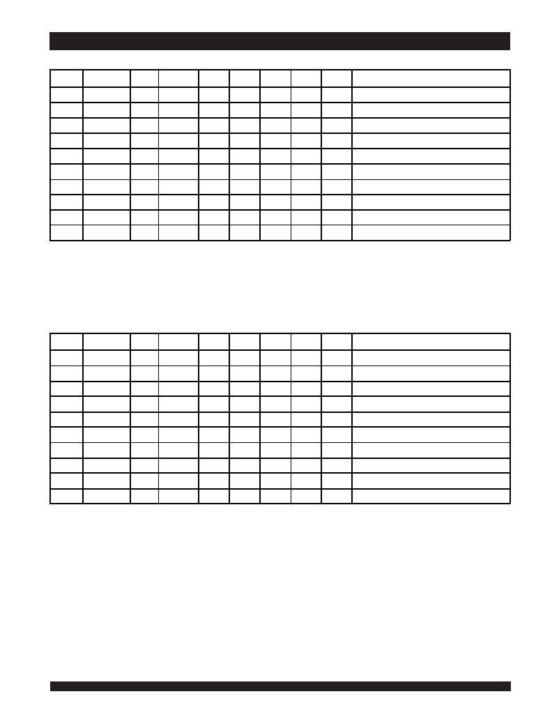
Read Operation with Chip Enable Used (1)
Cycle
n
n+1
n+2
n+3
n+4
n+5
n+6
n+7
n+8
n+9
Address
X
X
A 0
X
A 1
X
X
A 2
X
X
R/ W
X
X
H
X
H
X
X
H
X
X
ADV/ LD
L
L
L
L
L
L
L
L
L
L
CE (2)
H
H
L
H
L
H
H
L
H
H
CEN
L
L
L
L
L
L
L
L
L
L
BW x
X
X
X
X
X
X
X
X
X
X
OE
X
X
X
X
L
X
L
X
X
L
I/O (3)
?
?
Z
Z
Q 0
Z
Q 1
Z
Z
Q 2
Comments
Deselected.
Deselected.
Address and Control meet setup.
Deselected or STOP.
Address A 0 Read out. Load A 1 .
Deselected or STOP.
Address A 1 Read out. Deselected.
Address and control meet setup.
Deselected or STOP.
Address A 2 Read out. Deselected.
NOTES:
1. H = High; L = Low; X = Don’t Care; ? = Don’t Know; Z = High Impedance.
2. CE = L is defined as CE 1 = L, CE 2 = L and CE 2 = H. CE = H is defined as CE 1 = H, CE 2 = H or CE 2 = L.
3. Device Outputs are ensured to be in High-Z after the first rising edge of clock upon power-up.
Write Operation with Chip Enable Used (1)
5313 tbl 19
Cycle
n
n+1
n+2
n+3
n+4
n+5
n+6
n+7
n+8
n+9
Address
X
X
A 0
X
A 1
X
X
A 2
X
X
R/ W
X
X
L
X
L
X
X
L
X
X
ADV /LD
L
L
L
L
L
L
L
L
L
L
CE (2)
H
H
L
H
L
H
H
L
H
H
CEN
L
L
L
L
L
L
L
L
L
L
BW x
X
X
L
X
L
X
X
L
X
X
OE
X
X
X
X
X
X
X
X
X
X
I/O
?
?
Z
Z
D 0
Z
D 1
Z
Z
D 2
Comments
Deselected.
Deselected.
Address and Control meet setup.
Deselected or STOP.
Address D 0 Write in. Load A 1 .
Deselected or STOP.
Address D 1 Write in. Deselected.
Address and control meet setup.
Deselected or STOP.
Address D 2 Write in. Deselected.
NOTES:
1. H = High; L = Low; X = Don’t Care; ? = Don’t Know; Z = High Impedance.
2. CE = L is defined as CE 1 = L, CE 2 = L and CE 2 = H. CE = H is defined as CE 1 = H, CE 2 = H or CE 2 = L.
12
6.42
5313 tbl 20
发布紧急采购,3分钟左右您将得到回复。
相关PDF资料
IDT71T75902S85BGG
IC SRAM 18MBIT 85NS 119BGA
IDT71V016SA12PHGI
IC SRAM 1MBIT 12NS 44TSOP
IDT71V124SA10PHGI
IC SRAM 1MBIT 10NS 32TSOP
IDT71V256SA20PZG
IC SRAM 256KBIT 20NS 28TSOP
IDT71V25761S200PFGI
IC SRAM 4MBIT 200MHZ 100TQFP
IDT71V30L35TFI
IC SRAM 8KBIT 35NS 64STQFP
IDT71V321L25TFI
IC SRAM 16KBIT 25NS 64STQFP
IDT71V3556SA166BGGI
IC SRAM 4MBIT 166MHZ 119BGA
相关代理商/技术参数
IDT71T75802S200PFGI8
功能描述:IC SRAM 18MBIT 200MHZ 100TQFP RoHS:是 类别:集成电路 (IC) >> 存储器 系列:- 标准包装:45 系列:- 格式 - 存储器:RAM 存储器类型:SRAM - 双端口,异步 存储容量:128K(8K x 16) 速度:15ns 接口:并联 电源电压:3 V ~ 3.6 V 工作温度:0°C ~ 70°C 封装/外壳:100-LQFP 供应商设备封装:100-TQFP(14x14) 包装:托盘 其它名称:70V25S15PF
IDT71T75802S200PFI
功能描述:IC SRAM 18MBIT 200MHZ 100TQFP RoHS:否 类别:集成电路 (IC) >> 存储器 系列:- 产品变化通告:Product Discontinuation 05/Nov/2008 标准包装:84 系列:- 格式 - 存储器:RAM 存储器类型:SRAM - 同步 ZBT 存储容量:4.5M(128K x 36) 速度:75ns 接口:并联 电源电压:3.135 V ~ 3.465 V 工作温度:-40°C ~ 85°C 封装/外壳:119-BGA 供应商设备封装:119-PBGA(14x22) 包装:托盘 其它名称:71V3557SA75BGI
IDT71T75802S200PFI8
功能描述:IC SRAM 18MBIT 200MHZ 100TQFP RoHS:否 类别:集成电路 (IC) >> 存储器 系列:- 产品变化通告:Product Discontinuation 05/Nov/2008 标准包装:84 系列:- 格式 - 存储器:RAM 存储器类型:SRAM - 同步 ZBT 存储容量:4.5M(128K x 36) 速度:75ns 接口:并联 电源电压:3.135 V ~ 3.465 V 工作温度:-40°C ~ 85°C 封装/外壳:119-BGA 供应商设备封装:119-PBGA(14x22) 包装:托盘 其它名称:71V3557SA75BGI
IDT71T75902S75BG
功能描述:IC SRAM 18MBIT 75NS 119BGA RoHS:否 类别:集成电路 (IC) >> 存储器 系列:- 标准包装:1,000 系列:- 格式 - 存储器:RAM 存储器类型:SRAM - 双端口,同步 存储容量:1.125M(32K x 36) 速度:5ns 接口:并联 电源电压:3.15 V ~ 3.45 V 工作温度:-40°C ~ 85°C 封装/外壳:256-LBGA 供应商设备封装:256-CABGA(17x17) 包装:带卷 (TR) 其它名称:70V3579S5BCI8
IDT71T75902S75BG8
功能描述:IC SRAM 18MBIT 75NS 119BGA RoHS:否 类别:集成电路 (IC) >> 存储器 系列:- 标准包装:45 系列:- 格式 - 存储器:RAM 存储器类型:SRAM - 双端口,异步 存储容量:128K(8K x 16) 速度:15ns 接口:并联 电源电压:3 V ~ 3.6 V 工作温度:0°C ~ 70°C 封装/外壳:100-LQFP 供应商设备封装:100-TQFP(14x14) 包装:托盘 其它名称:70V25S15PF
IDT71T75902S75BGG
功能描述:IC SRAM 18MBIT 75NS 119BGA RoHS:是 类别:集成电路 (IC) >> 存储器 系列:- 标准包装:1,000 系列:- 格式 - 存储器:RAM 存储器类型:SRAM - 双端口,同步 存储容量:1.125M(32K x 36) 速度:5ns 接口:并联 电源电压:3.15 V ~ 3.45 V 工作温度:-40°C ~ 85°C 封装/外壳:256-LBGA 供应商设备封装:256-CABGA(17x17) 包装:带卷 (TR) 其它名称:70V3579S5BCI8
IDT71T75902S75BGG8
功能描述:IC SRAM 18MBIT 75NS 119BGA RoHS:是 类别:集成电路 (IC) >> 存储器 系列:- 标准包装:45 系列:- 格式 - 存储器:RAM 存储器类型:SRAM - 双端口,异步 存储容量:128K(8K x 16) 速度:15ns 接口:并联 电源电压:3 V ~ 3.6 V 工作温度:0°C ~ 70°C 封装/外壳:100-LQFP 供应商设备封装:100-TQFP(14x14) 包装:托盘 其它名称:70V25S15PF
IDT71T75902S75BGGI
功能描述:IC SRAM 18MBIT 75NS 119BGA RoHS:是 类别:集成电路 (IC) >> 存储器 系列:- 产品变化通告:Product Discontinuation 05/Nov/2008 标准包装:84 系列:- 格式 - 存储器:RAM 存储器类型:SRAM - 同步 ZBT 存储容量:4.5M(128K x 36) 速度:75ns 接口:并联 电源电压:3.135 V ~ 3.465 V 工作温度:-40°C ~ 85°C 封装/外壳:119-BGA 供应商设备封装:119-PBGA(14x22) 包装:托盘 其它名称:71V3557SA75BGI
